•
•
•
•
•
•
•

Design, fabrication, lithography, packaging and testing, and where India fits in the global chip supply chain
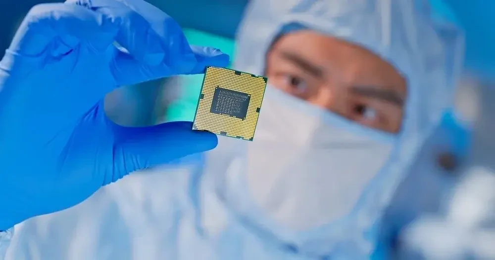
Semiconductor chips power everything from smartphones and cars to AI data centres and satellites. A single advanced processor can contain tens of billions of transistors, each far smaller than a virus. Making them is one of the most complex manufacturing processes humans have ever developed, involving hundreds of steps, ultra-clean factories and a global supply chain.
A semiconductor is a material whose electrical conductivity lies between a conductor (like copper) and an insulator (like glass). Silicon is the most widely used because it is abundant (derived from sand), stable and its conductivity can be precisely controlled by adding impurities, a process called doping.
The basic building block is the transistor, a tiny switch that turns current on and off, representing the 1s and 0s of digital logic.
India is a major hub for chip design talent, with many global semiconductor companies running large design centres in cities such as Bengaluru, Hyderabad and Noida.
Fabs are cleanrooms far cleaner than hospital operating theatres. Key repeated steps include:
Thin layers of materials such as silicon dioxide or metals are deposited onto the wafer.
A light-sensitive photoresist is coated on the wafer. Light shone through a patterned mask transfers the circuit design onto the resist. The most advanced chips use extreme ultraviolet (EUV) lithography, with a wavelength of 13.5 nanometres. The Dutch company ASML is the only maker of EUV machines, each costing well over a hundred million dollars.
Chemicals or plasma remove exposed material, carving the pattern into the layers.
Ions are implanted to change electrical properties in specific regions, forming transistors.
Layers of microscopic copper wiring connect billions of transistors.
These steps repeat dozens of times to build up many layers. Producing one advanced wafer can take around three months.
Companies that provide these services are called OSATs (outsourced semiconductor assembly and test).
Node names such as 5 nm, 3 nm and 2 nm were once linked to physical transistor dimensions. Today they are largely marketing labels for successive technology generations. A smaller node generally means more transistors per area, better performance and lower power, but the name is not a direct measurement.
| Segment | Leading regions |
|---|---|
| Chip design and EDA | United States, with growing design work in India |
| Lithography equipment | Netherlands (ASML), Japan |
| Advanced fabrication | Taiwan (TSMC), South Korea (Samsung), US |
| Memory | South Korea, US, Japan, China |
| Packaging and testing | Taiwan, China, Malaysia, and emerging hubs including India |
This concentration has made chips a strategic and geopolitical issue, with governments offering large subsidies to build domestic capacity.
Challenges include reliable power, huge volumes of ultra-pure water, specialised chemicals and gases, and experienced fab engineers.
They require extreme cleanliness, precision equipment such as EUV scanners and years of process development. Leading-edge fabs cost many billions of dollars.
A fab makes circuits on wafers; an OSAT packages and tests the chips after fabrication.
India has strong design capability and several packaging and fab projects under construction. Commercial-scale production is ramping up over the coming years.
From sand to smartphone, chipmaking combines physics, chemistry and engineering at astonishing precision. As demand surges for AI and electronics, countries including India are racing to secure a place in this critical industry.